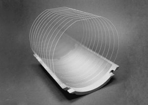
Optical Grade LiNbO3(LN) Wafer
Optical Grade LiNbO3 Crystal is widely used as frequency doublers for wavelength > 1μm and optical parametric oscillators (OPOs) pumped at 1064 nm as well as quasi‐phase‐matched (QPM) devices. Due to its large Electro‐Optic (E‐O) and Acousto‐Optic (A‐O) coefficients, LiNbO3 crystal is the most commonly used material for Pockel Cells, Q‐switches and phase modulators, waveguide substrate, and surface acoustic wave (SAW) wafers, etc.
Applications
1 ) EO Waveguide Phase Modulators 2 ) EO Waveguide Amplitude Modulators
3 ) Integrated Waveguide Photonics 4 ) Wave Guide Lasers
5 ) Polarizer for Optic Isolator 6 ) Quasi-phase Matching for SHG and OPO
Specifications
Material | Optical Grade LiNbO3 crystal | |
Curie Temp | 1142±2.0℃ | |
Cutting Angle | X-cut/Z-cut etc | |
Diameter/size | 3”/4” | |
Tol(±) | <0.20 mm | |
Thickness | 0.18 ~ 0.5mm or more | |
Primary Flat | 22mm/32mm | |
TTV | <3µm | |
Bow | -30<bow<30 | |
Warp | <40µm | |
Orientation Flat | All available | |
Surface Type | Single Side Polished /Double Sides Polished | |
Polished side Ra | <0.5nm | |
S/D | 20/10 | |
Edge Criteria | R=0.2mm or Bullnose | |
Optical doped | Fe/Zn/MgO etc for optical grade LN< wafers | |
Wafer Surface Criteria | Refractive index | No=2.2878/Ne=2.2033 @632nm wavelength |
Contamination, | None | |
Particles ¢>0.3 µ m | <= 30 | |
Scratch , Chipping | None | |
Defect | No edge cracks, scratches, saw marks, stains | |
Packaging | Qty/Wafer box | 25pcs per box |
